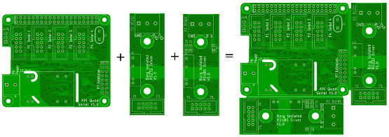
panelize.py is a tool I created a long time ago to panelize one of my kicad PCBs. Version 3 is a complete rewrite which supports kicad format 4 and 5 PCB files, those with the ending ".kicad_pcb". It can copy and optionally rotate and flip parts of PCB files. It can also be used to merge multiple PCB files. When PCBs are copied onto a "frame" PCB or prepared empty panel, the process can be repeated as often as needed. If changes are made to a source PCB the panelized PCB just has to be reassembled from all parts.
Download it from here, or get it directly from the subversion repository:
svn cat https://repos.borg.ch/projects/kicad/trunk/tools/panelize.py > panelize.py
The latest version is V3.1.6 (r998).
If you want to edit it and be able to view diffs, create patches, etc. use the following command to create a subversion working copy:
svn co https://repos.borg.ch/projects/kicad/trunk/tools panelize
Please send questions and patches generated using svn diff to mf@borg.ch.
The configfile contains all commands for the panelisation.
The config file is a simple text file. It contains one command per line. Empty lines and lines starting with # are ignored. Commands start with a keyword followed by the paramters. Strings can be enclosed in single or double quotes. All measurements are in millimeters.
Layer names:new
Creates a new empty destination PCB.
Example:
new
load filename
Loads a kicad PCB file and uses it as source for copies. If no destination PCB exists the loaded PCB is also used as destination.
Example:
load example.kicad_pcb
save filename
Saves the destination PCB to the specified file.
Example:
save example.kicad_pcb
compat 4.0.5
Save the PCB file in a version compatible to the specified version of kicad. Currently only the versions "4.0.5" and "latest" are supported.
Example:
save example.kicad_pcb
create-template
Creates a template from the source PCB and sets it as destination PCB. The template is a copy of the source containing all the configuration parameters, but no modules, traces, etc. are copied.
Example:
create-template
source-area X1 Y1 X2 Y2
Sets the rectangular area in the source PCB for copies.
Example:
source-area 50 50 74 100
exclude-layer layer-name
include-layer layer-name
include-layer all
Includes or excludes the specified layer from the copy. Multiple layers can be included or excluded by executing multiple include or exclude commands. Switching from include to exclude or vice versa clears the previous list.
Example:
exclude-layer Edge.Cuts
set-title text
set-date YYYY-MM-DD
set-rev text
set-company text
set-comment-1 text
set-comment-2 text
set-comment-3 text
set-comment-4 text
these commands set the texts in the title block.
Example:
set-title 'Panelized PCB'
clone-nets bool
When set to true the nets of the copies will be duplicated. Their names will have a prefix "C" followed by the number of the copy command and the original name. When nets are not cloned the resulting PCB will show a ratsnest for the missing connections between the PCBs.
Example:
clone-nets false
swap-internal-layers bool
When set to true internal layers will be swapped too when fliping a PCB. That means internal layer 1 becomes layer N, 2 becomes N-1, etc.
Example:
swap-internal-layers true
Copies the selected area to the given destination and optionally rotates it or flips it to the other PCB side. The coordinate is the upper left corner of the destination.
Example:
copy 76 50
Creates a grid of n-x times n-y copies of the source.
Example:
grid-copy 0 0 53 63 3 2
draw-line x1 y1 x2 y2 [layer-name [thickness]]
Draw a line. If layer or thickness are not specified a default is used.
Example:
draw-line 75 50 75 100
draw-line 75 50 75 100 Eco1.User 0.5
draw-text text x y [angle [layer-name [height [width [thickness]]]]]
Draw some text. For the arguments which are not specified a default is used.
Example:
draw-text horizontal 75 105
draw-text vertical 90 105 90 Eco1.User 3 2 0.25
set-layer layer-name
Sets the layer name which is used as default for the draw commands.
Example:
set-layer Eco1.User
set-line-thickness thickness
Sets the thickness which is used as default for the draw-line command.
Example:
set-line-thickness 0.3
set-text-font
Sets the font (charater height and width, line thickness) which is used as default for the draw-text command.
Example:
set-text-font 1.5 1.2 0.15
load example.kicad_pcb
source-area 50 50 74 100
copy 76 50
save panelized.kicad_pcb
# options
clone-nets true
exclude-layer Edge.Cuts

# rpi-quad-serial-panel-border: 54.5/54.5..119.5/110.5
load rpi-quad-serial-panel-border.kicad_pcb

# rpi-quad-serial: 54.5/54.5..119.5/110.5
load rpi-quad-serial.kicad_pcb
source-area 54.4 54.4 119.6 110.6
copy 54.4 54.4
include-layer Edge.Cuts
source-area 66 87 102 109
copy 66 87
exclude-layer Edge.Cuts

# ttl-2-rs232-isol.kicad_pcb: 89/88..111/150
load ttl-2-rs232-isol.kicad_pcb
source-area 89 88 111 150
copy 121 54.5

# ttl-2-rs485-isol.kicad_pcb:
load ttl-2-rs485-isol.kicad_pcb
source-area 89 88 111 150
rotate-right 54.5 112

# save...
save rpi-quad-serial-panel.kicad_pcb
KiCad PCB Panelization with Javascript is a script that generates empty M*N panels. PCB's can be manually copied into these panels, or using panelize.py. Here is an example script to copy 3*2 PCBs with 50*50mm size:
load my-50x50mm-pcb.kicad_pcb
create-template
exclude-layer Edge.Cuts
source-area 120.62 80.85 170.658 130.888
grid-copy 0 0 53 53 3 2

load generated-panel.kicad_pcb
include-layer all
source-area -100 -100 1000 1000
copy -100 -100

save panelized.kicad_pcb